4 Layer Laminate Package Ic

Fr 4 Laminate 4 Layer Hasl Multilayers Pcb With Images Pcb Board Circuit Board Printed Circuit Board

Mis Packaging Takes Off

High Frequency Pcb Used Rogers Duroid Rt 5880 Material With Er Dk 2 2 In 2020 Chinese New Year Holiday Pcb Design Laminates

Hdi Pcb Are Utilized To Meet The Customer Demand For Complex Designs In Smaller Form Factors Across Th Circuit Board Insulation Materials Printed Circuit Board

Fuji Prescale 4lw Helps Map Lamination Tactile Pressure Range In Manufacturing Microfluidic Structures Tactile Manufacturing Helpful

Pet Pouch Thermal Laminating Film Used As Protective Layers For Important And Frequently Paper File Hot Foil Stamping Foil Stamping Plastic Film

Laminate is constructed in layers to create lasting affordable beautiful floors.
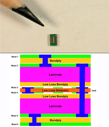
4 layer laminate package ic. No matter how hard you push on it when you mount it to the package those bumps aren t going to dig down through the laminate layers of the package. The pad pitch is 120μm with an 80μm pad size. There are a variety of ways to categorize ic packages based on formation. Some package types have standardized dimensions and tolerances and are registered with trade industry associations such as jedec and pro electron.
The line space specs are 10μm and above. Design flows are not able to address multiple technology designs ic laminate package and pcb need to be designed together em interactions between substrates need to be modeled and accounted for the need to move from disjointed tools design flows to. Additionally a category for wafer ic assembly known as wafer level packaging wlp has caught on in industry parlance. As such there are two types of ic packages.
Four reasons to avoid multi layer flip chip pin padstacks. The lead frame type and the substrate type. Multi technology examples 2. Illustrate with few applications single chip module multi chip module flip chip solder bumps module transceiver module electro thermal simulation 5.
A very large number of different types of package exist. Improve electrical performance and incorporate higher ic functionality amkor flip chip bga fcbga packages are assembled around state of the art single unit laminate or ceramic substrates. The pins can be placed on top of vias which connect to objects on other layers but the pins themselves cannot do so. Four layers of material each of which has its own purpose are fused together through a direct pressure process that binds them into one extremely durable material.
Ic laminate package multi technology pa module design agenda 1. Utilizing multiple high density routing layers laser drilled blind buried and stacked vias and ultra fine line space metallization fcbga. These laminates feature superior versatility and come with excellent properties that make these suitable for wide variety of packaging applications. Semiconductor device fabrication is the process used to manufacture semiconductor devices typically the metal oxide semiconductor mos devices used in the integrated circuit ic chips that are present in everyday electrical and electronic devices.
Ic laminate package multi technology module design challenges. It is a multiple step sequence of photolithographic and chemical processing steps such as surface passivation thermal oxidation planar. Improved design methodology 4. In sesub the most common configuration is an embedded package in a 4 layer substrate but some are developing 2 5 and 6 layer options.

Laminate Fr4 Pi Board Thickness 1 57mm Copper Thickness 17 5um Hoz Solder Resist Green Color Surface Finish Immersion Flex Printed Circuit Boards Layers

Embedded Die Packaging Emerges
Capabilities Of Multi Layer Organic Packaging

Rf Pcb High Frequency Pcb Made From Polytetrafluoroethylene Ptfe Pcb Ceramic Filled Fluoropolymer Or Ceramic Fi Printed Circuit Board Circuit Board Graphic

Searching For Pcb Fabrication Supplier What Should They Offer Printed Circuit Boards Substrate Printed Circuit

Advanced Ic Packaging A Technology Overview Ppt Video Online Download
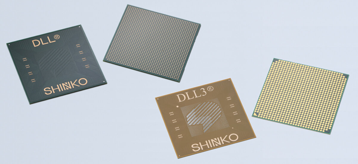
Build Up Substrate Services Shinko Electric Industries Co Ltd

The Carmick Products Card Id Preserver The Secret To Keeping Your Confidential Information Where It Belongs Rfid Blocking Consumer Marketing Prevention Rfid

4 Layer Hasl With Gold Finger Purple Soldermask Color Pcb Circuit Board Printed Circuit Board Printed Circuit Boards

Halogen Free Pcb There Is Increasing Demand For Environmentally Friendly Pcb Electronic Products Halo Printed Circuit Board Circuit Board Electronic Products

Pcb Or Printed Circuit Board Is A Mechanical Assembly That Consists Of Etched Copper Patterns Lami Printed Circuit Board Electronic Circuit Board Circuit Board

Global Laser Direct Imaging Ldi Equipment Market Research Report 2019 Market Research Growth Strategy Marketing

Pin On Mighos

